
● ISA Bus
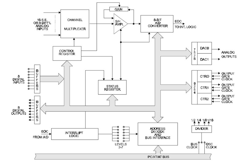
● No. of Channels: Eight differential or 16 single-ended inputs.
● Voltage Ranges: Software selectable, ±128 mV or 0-255 mV w/1 mV resolution, ±5V or 0-10V w/39 mV resolution.
● Overvoltage Protection: ±40 VDC, single channel.
● Input Impedance: 10 Megohm
● Accuracy: ±0.4% ±1 count.
● Linearity: ±1 count.
● Resolution: 8 bit binary.
● Temperature Coefficient: Zero and gain stability each ±1 LSB over full operating temperature range.
● Throughput: 16,600 conversions/second maximum.
● No. of Channels: 2
● Output Voltage Range: ±10 VDC.
● Resolution: 8 bit binary.
● Output Load: 5 mA maximum.
● Accuracy: ±0.4% ±1 bit.
● Inputs
- No. of Inputs: 8 TTL- and switch-compatible.
- Inputs pulled up to +5 VDC by 1 Kilohm resistor.
- Logic Low: 0 to 0.4 VDC.
- Logic High: 2.4 to 24 VDC.
● Outputs:
- No. of Outputs: 8, TTL/DTL compatible. Outputs are tri-stated at power on and at reset. Zener diode protected at 5.6 VDC.
- Logic Low: 0 to 0.4 VDC at 24 mA sink current
- Logic High: 2.5 to 5.0 VDC at 10 mA source current.
● Level: Jumper selectable, levels 2-7.
● Enable/Disable: Interrupt generated by completion of A/D conversion. Interrupt cancelled when A/D data are read or when there is a computer write to base address plus 1 (reset interrupt request).
● No. of Counters: Three independent, 16-bit, fully programmable.
● Clock: Either internal derived from computer clock (or color oscillator frequency) divided by 1/2, 1/4, 1/8, or 1/16 or from external clock source.
● Drive Capability: 5 LSTTL loads. (2.2 mA at 0.45 VDC).
● Input Load (Gate and Clock): ±10 mA, TTL/CMOS compatible.
● Input Clock Frequency:10 MHz max.
● Active Count Edge:Negative edge.
● Clock Pulse Width: 50 nSec high / 50 nSec low min.
● Operating Temperature Range: 0° to 60°C.
● Storage Temperature Range: -40° to +100°C.
● Humidity: 0 to 90% RH, non-condensing.
● 13.1 inches (333mm), plugs into a “l(fā)ong slot” in PC
● +5 VDC at 500 mA.
● +12 VDC at 20 mA.
● -12 VDC at 20 mA.
● This product is designed to be in full compliance with CE requirements.