

● PCI Bus
● Resolution: 12 bits (0 to 4095 decimal)
● Channels:
- PCI-DA12-2: Two independent or simultaneous update
- PCI-DA12-4: Four independent or simultaneous update
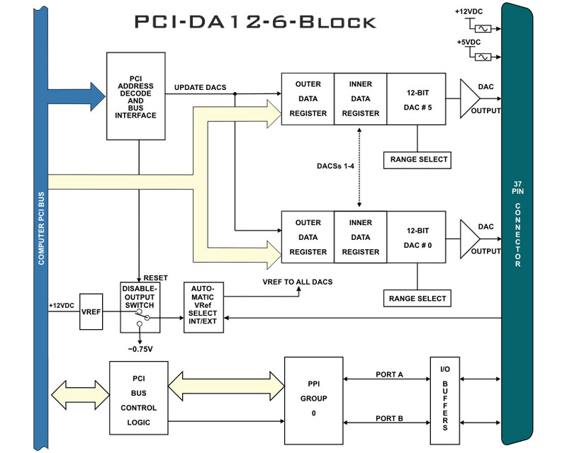
- PCI-DA12-6: Six independent or simultaneous update
- PCI-DA12-8: Eight independent or simultaneous update
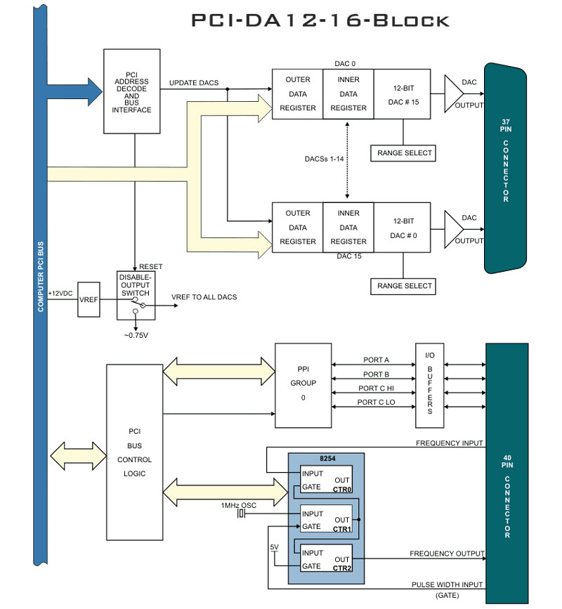
- PCI-DA12-16: Sixteen independent or simultaneous update
● Voltage Output Ranges:0-2.5 VDC, 0-5 VDC, 0-10 VDC, + 2.5 VDC, + 5.0 VDC, + 10.0 VDC
● Current Range: 4 to 20 mA (with external excitation voltage of 8-36VDC)
● Short-circuit Current: 25 mA maximum
● Output Drive Capability: 5 mA maximum
● Output Resistance: Less than 0.1 ohm
● AD7237 monolithic chip, double buffered
● Relative Accuracy: ± 4 LSB max, ± ? LSB typical
● Linearity: + ? LSB integral non-linearity over rated temperature range
● Monotonicity: 12 bits over operating temperature range
● Settle time: 8 usec to 1 LSB for full-scale step input
● Data Format: 12-bit binary, right justified and offset binary for bipolar outputs
● Gain Stability: + 15 ppm/°C typ.
● Data Format: Right-justified, two bytes (8LSB’s and 4MSB’s)
● Type: 82C54-5 programmable interval counters.
● Output Drive: 2.2 ma at 0.45 VDC (5 LSTTL loads).
● Input Gate: TTL/DTL/CMOS compatible.
● Clock: On-board, 1 MHz crystal-controlled clock.
● Active Count Edge: Negative edge.
● Min Clock Pulse Width: 30nS high/50nS low.
● Timer Range: 48 bits
● Operating Temperature: 0 to +60o C
● Storage Temperature: -20 to +85o C
● Humidity: 0 to 90% RH, non-condensing.
● Size:
- PCI-DA12-8/16: 12.2″ (310 mm) long
- PCI-DA12-2/4/6: 6.0″ (152 mm) long
● Inputs:
- Logic High: 2.0 to 5.0 VDC.
- Logic Low: -0.5 to +0.8 VDC.
- Input Load (High): +20 μA.
- Input Load (Low): -200 μA.
● Outputs
- Logic High: 2.0 VDC min., source 32 mA.
- Logic Low: 0.55 VDC max., sink 64 mA.
● +5 VDC at 500 mA is available on the 37-pin connector.
● This product is designed to be in full compliance with CE requirements.